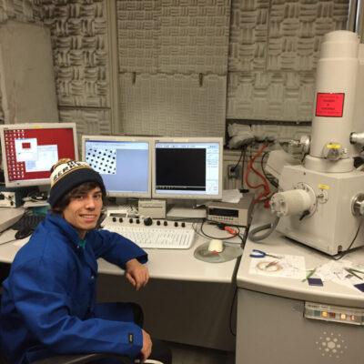
Joey Barreto Rose Hills
Electronic Transport in NbSe2-NbSe3 van der Waals Heterostructures
Today’s technology has allowed for significant advances in the fields of condensed matter physics and materials science. In recent years scientists have been able to consistently isolate high quality, atomically-thin layers of various crystals and compounds, beginning with graphene (a single sheetof carbon in a hexagonal pattern) in the mid-2000s. While there has been much research into the properties of single layers of certain materials, a rich variety of novel phenomena can explored in stacks of these layers, known as van der Waals heterostructures. The customization of these stacks and the ability to tune their properties make them an exciting test bed for both validating theories and improving electronic devices.
Previous work in my lab has contributed to a good repository of metallic crystals, and I propose to construct heterostructures from thin samples of these crystals, starting with niobium diselenide (NbSe2) and niobium triselenide (NbSe3). Motivation for such research stems from the exotic electronic properties of these materials: NbSe3 exhibits two sliding charge density waves, and NbSe2 both a charge density wave and superconductivity. Superconductivity is a highly sought-after phenomenon where below a certain temperature, a material permits the flow of electricity without offering any resistance, and expels all (or some) of an external magnetic field. A charge density wave is another kind of collective electronic behavior, a periodic modulation in the density of electrons in a material, and comes in two kinds, sliding and static, depending on the purity of the sample. It is unknown how these collective phenomena will interfere at the NbSe2-NbSe3 junction, and this gap in knowledge is what I seek to fill.
Message To Sponsor
I am very grateful to the Rose Hills Foundation for their generous support, which has allowed me to devote myself full-time to research this summer. The experience that I shall gain will definitely give me a taste of academia and familiarize me with the entire proposal-to-publication pipeline. I intend for my work to contribute to a senior thesis and help guide the direction of my future interest and research.